Home

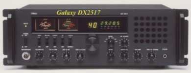
Galaxy DX-2517

CHASSIS EPT690010Z

CHASSIS EPT069610Z


WINScanner

WINScanner with single Off-set oscillator

WINScanner with dual Off-set oscillator


Block Diagram

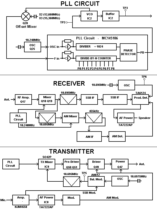
EPT690010Z Block Diagram
PLL CIRCUIT
The Phase Lock Loop (PLL) circuit is responsible for developing the receiver’s first local oscillator signal and the transmitter’s exciter signal. The PLL circuit consists primarily of IC2, IC3, IC4, IC5, Q25, Q27, Q28, Q29 and Q61. The PLL circuit is programmed by the user’s rotary channel switch. The switch allows rorary channel switch to communicate the correct binary data information to the programmable divider inside of IC3. IC3 then controls the VCO (Voltage Controlled Oscillator), to oscillate on the correct frequency. This signal is fed either into the receiver’s first mixer (for receive operation) or the transmitter’s mixer (for transmit operation).

RECEIVER CIRCUIT
The incoming receive signal come into the radio via the antenna and into the front end pre-amp consisting of Q17. The RF signal is fed into the mixer circuit of the Q18 & Q19 and then into the AM IF section of the receiver (depending on the mode of operation). The signal is then detected by either the AM detector or product detector and then fed to the audio amplifier section of the receiver and finally out to the speaker.

TRANSMITTER MODULATION CIRCUIT
The transmitter modulation circuit modulates the low level RF signal from the PLL exciter circuit with the user’s audio voice signal from the microphone. The audio from the microphone is then amplified and fed into the transmit amplifier circuit.

If the transceiver is in the AM mode, the AF power amplifier modulates the last RF amplifier, which produces a true amplitude modulated RF signal.

TRANSMITTER AMPLIFIER CIRCUIT
The transmitter takes the basic exciter signal from the TX mixer and amplifies it through a series of amplifiers consisting of Q50, Q51, Q49, Q47 and Q48 where it is sent out to the antenna connector.

Adjustment

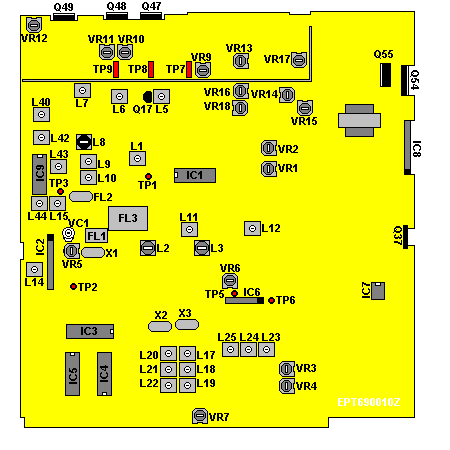
EPT690010 PCB

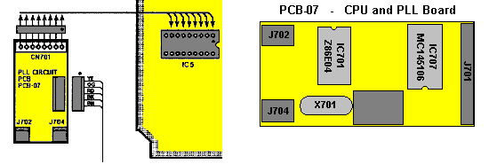
PLL and CPU PCB
In some model`s (with CHASSIS EPT069610Z) the PLL-circuit on Main PCB is replaced by a separate CPU and PLL board.
CPU and PLL PCB

Test equipment required:
Power Supply: 13,8 VFrequency CounterDummy Load 50 ohmOscilloscope
DC AmperemeterRF SSGAF SSG

Preparation alignment:


ClarifierMid.
SQ GAINMax.
AF GAINMax.
RF GAINMax.
MIC GAINMax.
MOD, S/RFS/RF
NB/ANLOff
Reading PointConditionAdjustmentProcedure
PLL
Vonnect Voltmeter to TP2.
Connect Oscilloscope to TP3.
G-band Ch. 40
AM RX-mode
L14
L15
6,5V +/- 0,1V
Connect FrequencyCounter to TP5.G-band Ch. 1
AM RX-mode
L2310,695MHz +/- 20Hz
OSCILLATOR
Connex CX4400:
Connect FrequencyCounter to TP3.G-band Ch. 40
AM RX-mode
L1718,890MHz +/- 20Hz
Connect FrequencyCounter to TP3.E-band Ch. 1
AM RX-mode
L2017,550MHz +/- 20Hz
Connect FrequencyCounter to TP3.G-band Ch. 1
AM TX-mode
L2018,890MHz +/- 20Hz
RECEIVER
RF SSG to antenna jack.
28,915MHz
1uV output
30% modulation
F-band Ch. 19
RX AM-mode
L2, L3,
L4, L5,
L6, L7,
L8, L9,
L10
Maximum at audio output
RF SSG to antenna jack.
28,245MHz
1uV output
30% modulation
B-band Ch. 1
RX AM-mode
L5,
L6,
Maximum at audio output
RF SSG to antenna jack.
29,585MHz
1uV output
30% modulation
G-band Ch. 40
RX AM-mode
L5,
L6,
Maximum at audio output
RF SSG to antenna jack.
28,915MHz
100uV output
3kHz deviation
F-band Ch. 19
RX FM-mode
L4Maximum at audio output
RF SSG to antenna jack.
28,915MHz
0,5uV output
Modluation off
Connect Voltmeter to TP3
F-band Ch. 19
RX AM-mode
NB-ANL ON
L1DC voltage to maximum
RF SSG to antenna jack.
28,915MHz
0,5uV output
30% modulation
F-band Ch. 19
RX AM-mode
NB-ANL ON
VR3Adjust until squelch just open
RF SSG to antenna jack.
28,915MHz
0,5uV output
30% modulation
F-band Ch. 19
RX AM-mode
VR1Adjust internal meter to "S9"
TRANSMITTER
Connect RF-Power meter to antenna jackF-Band Ch. 19.
AM TX-mode
L40, L42,
L43, L44
Maximum power
Connect RF-Power meter to antenna jackF-band Ch. 19
AM TX-mode
VR9RF Power meter
Connect Oscilloscope to antenna jackF-band Ch. 19
AM TX-mode
VR1695% AM-modulation
Connect Deviation meter to antenna jackF-band Ch. 19
FM TX-mode
VR54kHz FM Deviation
Connect RF-Power meter to antenna jackF-band Ch. 19VR14
VR18
High power
Low power

Microphone Connection

PinDescription
1Ground
2Microphone
3TX Key (Connect to Ground)
4Speaker (Connect to Ground)

COMPONENTS

Connex CX-4400 Schematic Diagram
Connex CX-4400HP Schematic Diagram
MC145106P PLL Frequency Synthesizer
S042P TX Mixer
KIA6410S Oscillator, Mixer and Amplifier
uPC1028H FM IF Amplifier and Detector
AN612 Balanced SSB Modulator
TA7222 Audio Power Amplifier
NJM4558 Dual Operational Amplifier
TA6324 Quad Operational Amplifier
2SC1969 RF Finale Transistor
2SC2312 RF Finale Transistor
2SC2166 RF Driver Transistor
2SC2086 RF Pre-Driver Transistor

Improved receive gain

Quieting of AM reception and improving gain of incoming signals is a common request from radio operators. In the first stages of the HF input 2SC1674 transistor can be found. This transistor is responsible for the amplification of a small detected signals. A problems exist if the transistor itself is noisy as is such the case of the 2SC1674 when compared to other low noise packages. Along with the amplification of the incoming signals is transistor noise. Replacement of this transistor with a higher gain, lower noise transistor greatly improves the signal to noise ratio of your receiver.
We will use an 2SC2999 transistor that has higher gain lower noise characteristic. Replace the 2SC1674 (TR17) with an 2SC2999 (or similar low noise and high gain transistor) to achieve this improved signal to noise ratio.
Re-Adjust L5 and L6
The gain will improved with more than 6dB with the same signal to noise ratio.